Material technology stands with a massive scope since everything in the universe is made out of materials. Consciously or unconsciously every living being is related to materials since they too are created in the form of a bio material. In order to meet the requirements extensively materials being used globally where they could be pure materials or composite materials which could be naturally occurring or manmade.
On the other hand, modern industries would not have a chance without material-related technologies. In industrial usage, especially metals, are exposed to severe conditions depending on requirements such as high temperatures, high pressures, low temperatures, and chemically reactive environments to put forth their abilities to their extremes. Whatever the application, it is very important to test the metal composition of a composite since the inherited characteristics of individual elements may influence the overall characteristic of a composite material. In diagnosing materials, tracking metal composition is also a huge area that has created a demand in both the industry and research. Sometimes, even though we name a specific material by its name, that might refer to the major component, which is called the base material. The question is how much of the base actually exists in the given material and what other alloys remain in relation to its percentage.All these come under metallurgy, where metallurgy is considered as a domain of materials science and engineering that studies the physical and chemical behavior of metallic elements, their inter-metallic compounds, and their mixtures, which are called alloys.
There are many different alloy compositions, each with their own set of specific properties. Certain alloys of the same base metal composition can often have different properties. For example the resistance of stainless-steel alloys to corrosion under acidic environments could make several steel alloys highly resistant to certain acids whereas some are not. Selection of the inaccurate grade may result in unexpected failure. In that case it is vital to measure the composition of a metallic alloy and usually several techniques are available to trace elemental analysis.
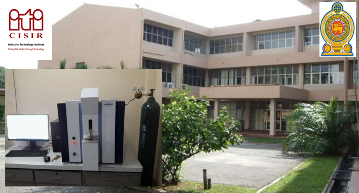
Apart from the popularly known method of X-ray fluorescence spectroscopy (XRF), the latest high-tech instrument is now in town at the Industrial Technology Institute (ITI) Colombo 7. The newly commissioned Advanced CCD Optical Emission Spectrometer at the Materials Laboratory (ML) of ITI has already started providing services to the industry for almost one year, making a fair return on investment.
What is this technology?
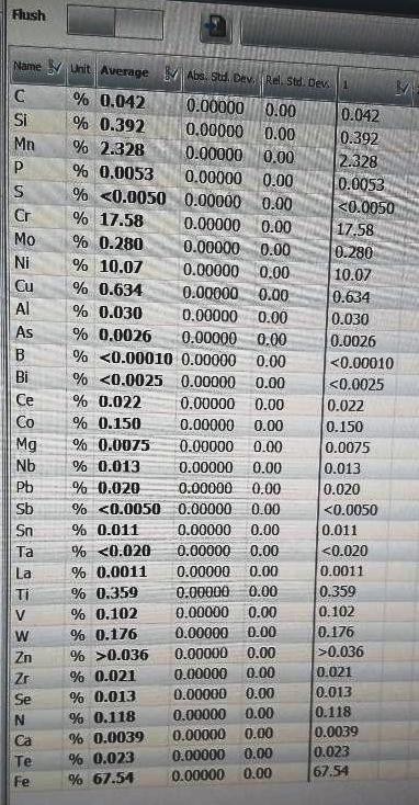
Optical Emission Spectrometers are capable of tracking elemental alloys at tracer levels of parts per million (PPM).
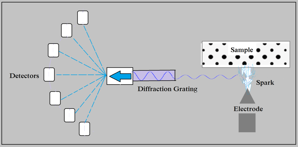
A method, also known as “arc-spark,” is a method that uses an arc or a spark, where an arc is similar to a lightning on-off and a spark is a series of multi-discharge.A high electric voltage is applied between an electrode and a sample located a few millimeters away, resulting in an electrical discharge (Arc-spark).
As a result, the electrical discharge will heat up to several thousand degrees Celsius and vaporize the surface material to make an electron (photon) excitation.
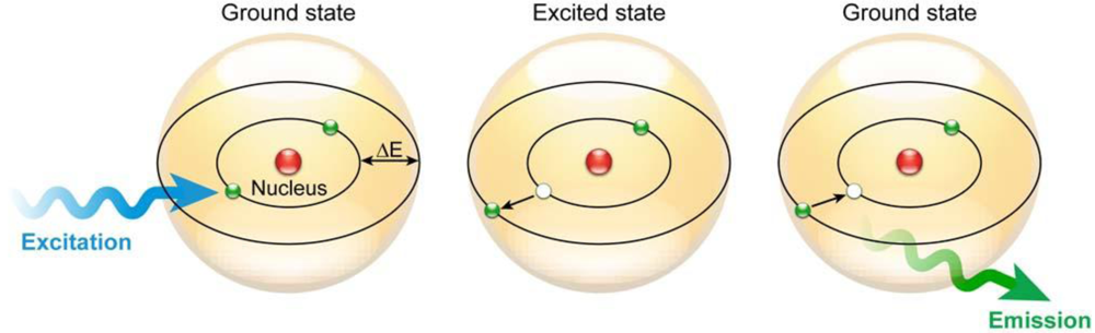
Image: https://socratic.org/questions/5723851511ef6b7fe53db9e4
The energy of electrical discharge makes the electrons in the outer shell eject due to the energy abortion since they are less tightly bonded and further away from the nucleus. As a result, the atom becomes unstable, and the vacancies left by the ejected electrons are filled by electrons from further away, re-emitting energy.
The released energy of multiple optical emissions from the vaporized sample, known as plasma, passes on to a spectrometer where a diffraction grating in the spectrometer separates them into specific wavelengths, identifying elements. Detectors measure the intensities of light for each wavelength, as the intensities are proportional to the concentrations of the elements. Here, the peak area corresponds to the quantity.
It should be reminded that the type of plasma depends on both the measurement accuracy and element measured.
It is the computer system which acquires the measured intensities and processes those data by following a predefined calibration. Having said that, this instrument is capable of producing the elemental composition within 3 to 30 seconds.
Optical emission spectroscopy (OES) involves the collection, spectral dispersion, and detection of light. Because OES from plasmas is often very strong. However, efficient detection is needed and rapid analysis is important and only a small fraction of the surface will be subjected for processing.
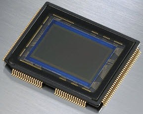
The instrument commissioned at ITI is armed with highly sensitive photon detectors called charged coupled detectors (CCD). These are the detectors that can be divided into a large number of light-sensitive small pixels. It is a silicon-based multi-channel array detector of UV, visible, and near-infra light. An integrated circuit is etched onto a surface made with silicon to form light-sensitive elements called pixels. Striking photons on the surface generate charges that could be traced by electronics and turned into a digital copy of the light patterns.
This method requires Argon gas becoause of a unique reason. Argon gas is an important analytical condition for the arc-spark optical emission spectrometer. It is crucial for normal use and accurate results. Usually, 99.999% purity is required for Argon gas. The gas creates isolated environments, assisting excitation since it separates elements such as oxygen and nitrogen from the air.
In the detection, oxygen absorbs most of the elemental lines and is also easily affected by external nitrogen elements, resulting in instability and producing erroneous results. Argon helps to avoid this situation. The chamber is filled automatically with argon, which also ensures the cleanliness of the optical chamber and avoids the deviation caused by the detection of ultraviolet elements. At the same time, argon gas helps clean the spark chamber of the excitation chamber and remove the exhaust gas.
Commissioned instrument at ITI
Domestic industrial applications require metal composition testing as well as maintaining quality standards and verifying metal grades. For example, electrical conductors used for lightning protectors require 99.99 pure copper, while high-purity aluminum is used in a wide range of applications such as the electronics industry, capacitor foil manufacturing, producing high-purity alumina, fabrication applications, manufacturing of flat panel and liquid crystal displays (LCD), and medical and cosmetic applications.
This analytical testing instrument is the one and only high-tech instrument found so far in Sri Lanka with the advantage of being able to detect up to 99.99 purity, reduce lead time, reduce labor hours, and lower operational costs. Apart from that, some of the standard testing requires the oxygen and nitrogen levels to produce the standard testing report, and thanks to the Advanced CCD Optical Emission Spectrometer, the standard reports in this area are not a nightmare any more. Iron and steel and its alloys, aluminum and its alloys, copper and its alloys, nickel and its alloys, cobalt and its alloys, magnesium and its alloys, lead and its alloys, tin and its alloys, titanium and its alloys, zinc and its alloys are some of the materials that the machine is recommended for.
ITI expects to acquire accreditation in near future with the new commissioning.
Acknowledgement: Dr. H P P S Somasiri, Mr. Kosala Amaranayake
Reference