In material science a common insitu method of analyzing the surface morphology of a sample is by using a scanning electron microscope. A Scanning Electron Microscope (SEM) analyses the surface of a given sample well beyond optical microscope usage. It is a very useful technique in the materials characterization with the advantage of incorporating very little sample amounts and also it is a non-destructive technique which implies that the samples will not be damaged and could be recovered. The electrons interact with atoms in the sample, producing various signals that contain information about the surface morphology and composition of the particular sample.
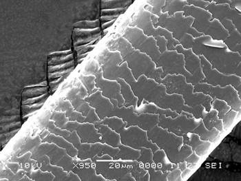
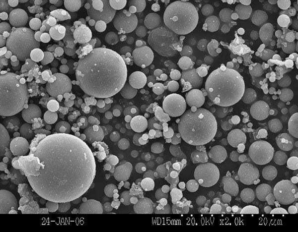
The only requirement for this technology is that the sample must be conductive, since the method has to have interactions with the electrons emitted by the equipment and the sample. If not a sample metallizer could be used on non-conductive samples to get them conductive by depositing a few nanometer layer to get the sample conductive by means of physical vapor deposition, mainly gold particles are commonly used in this regard. SEM produces High resolution images. It allows us to know what type of surface topology our sample has, its defects and its composition.
The resolution of modern SEMs is of the order of 2 nm. This compares with a resolution of about 1 mm for a conventional optical microscope. However it is to be said that the next type of electron microscope which is the transmission electron microscope (TEM), in which electrons pass through a very thin sample, has a higher resolution compared to the SEM (~ 0.1 nm). Individual atoms could be imaged with a TEM but not with a SEM.
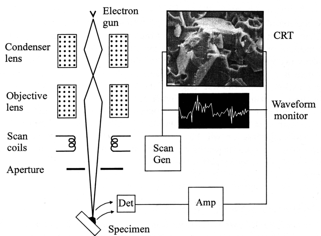
Basically a heated cathode filament feeds with a voltage difference produces an electron beam and is accelerated through another voltage difference (averaging around 5-20KV) towards a center hole anode enabling minus charged electrons to run through. It is then directed at the surface of the sample. As the sample collides with the electron beam the minus electrons are scattered and will be collected using a plus charged detector where then it will be photo multiplied before feeding it to the computer system. Some use photo scintillators. Different types of detectors are used to capture different types of signals generated after the electron collation. The electron beam uses a rectangular scanning pattern called razor scanning to scan a specific location of a sample. The actual size could be magnified up to may be 30,000 or more with an SEM and nano scales too could be achieved with modern SEMs.
The two other main components located in between the sample and the gun happens to be the Condenser lenses and radial scanning coil. The scanning coil delivers electromagnetic data as a secondary feed to the computer system. SEM must be carried out under vacuum conditions, where mostly two chambers are employed with the vacuum status. To insert samples the vacuum should be released with air and samples holders which carries samples are located inside before turning on the vacuum pumps. This is done mainly because of the reason that the electrons hesitates to travel through air.
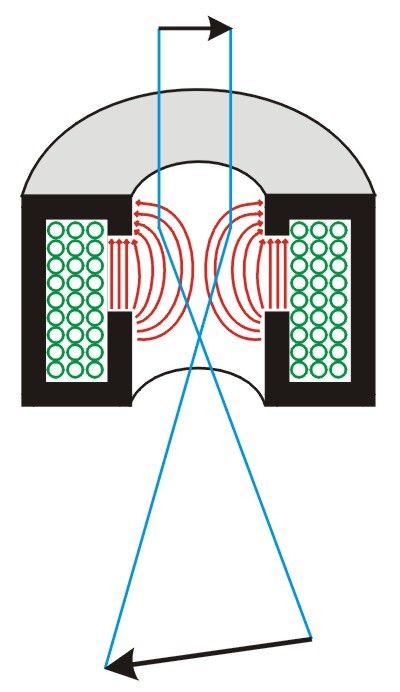
Condenser renders a divergent beam from a point source into a parallel or converging beam to illuminate an object. All modern SEMs use electromagnetic lenses. These consist of a coil of copper wires inside iron pole pieces. Solenoid of wire together with a magnetic pole piece creates and concentrates a magnetic field.
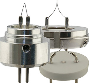
The standard filament of an SEM electron gun is mostly the tungsten filament used due to its low cost however Lanthanum hexaboride (LaB6) and Cerium hexaboride (CeB6) filaments are also available associating higher costs.
Types of signals scattered after electron collide with the sample
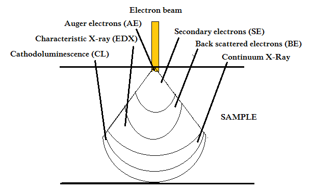
A basic SEM produces two main types of signals named as back scattering signal and the secondary signal.
Secondary Electrons (SE)
Unlike BSEs, SEs originates from the surface or the near-surface regions of the sample. They are a result of inelastic interactions between the primary electron beam and the sample which got lower energies than the backscattered electrons. Secondary electrons are very useful for the inspection of the sample surface topography .
Backscattered Electron Imaging (BSE)
BSEs come from deeper regions of the sample, whereas SE originates from surface regions. BSE images show high sensitivity to differences in atomic number; the higher the atomic number, the brighter the material appears in the image. SE imaging can provide more detailed surface information.
BSEs originate from a broad region within the interaction volume. They are a result of elastic collisions of electrons with atoms, which result in a change in the electrons’ trajectories.
When electrons collides with larger atoms much stronger electrons scatters compared to light atoms, which produces a higher signal. The number of the backscattered electrons reaching the detector is proportional to their atomic number. This dependence of the number of BSEs on the atomic number helps us differentiate between different phases, providing imaging that carries information on the sample’s composition. BSE images can also provide valuable information on crystallography, topography, and the magnetic field of the sample.
However depending on the additional SEM facility further signals from deeper layers could capture other information as depicted below
X-ray detector (EDX, EDS or EDAX)
These detectors capture the energy from the X-rays generated on the surface (third layer of the ‘pear’) and they are characteristics of each element of the sample so they provide us with information about elemental composition. Unlike the BSE, they provide us with more information on the sample allows us to know in a semi-quantitative way the composition of the surface of our sample.
X-ray Detector (WDS)
Similar to EDX, but instead of receiving the energy of all X-rays at once, it only measures the signal generated by a single element. It is a slower but more sensitive and precise technique.
Diffracted backscattered electron detector (BSED)
This detector receives the energy of electrons diffracted by the surface that comply with Bragg’s law and provide information on the crystal structure of the sample
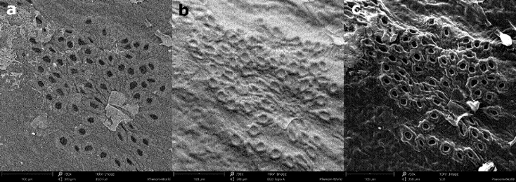
(a) SE Detector (b) back scatters (c) BSE Detector (Image – https://www.thermofisher.com/blog/microscopy/sem-signal-types-electrons-and-the-information-they-provide/ )Differences of SEM, FE-SEM or FIB-SEM
SEM: Conventional SEMs have a thermal source of electrons.
FE-SEM (field emission SEMs): They have electron source with a field emission gun to provide the high and low energy electron beams. Much focused beams allow better resolution.
Dual Beam/ FIB-SEM (double beam microscope or focused ion beam SEMs): This has two columns, one of ions and the other at 52º of electrons.The ion column uses a Gallium (Ga +) ion beam. Ga + ions are 130,000 heavier than electrons, so the interaction with the sample is stronger although its penetration is less. Additionally, ion slices can be made to visualize the inner layers
Applications of Electron Microscopy
Product design failure analysis: To know why a failure has occurred, for example is it a fatigue force that appeared to brake of a metal rod. The morphology and composition of defects that appeared in the quality tests of a product could be characterized. Another type of failure that can be studied are delaminations (material fractures into layers) and adhesion (tendency of dissimilar particles or surfaces to cling to one another).
Characterization of surface texturing: When the topography and structure that has been generated wants to be known
Analysis of surface defects and quality control: by means of the SEM it is possible to visualize the defects, to know the typology, for example the defects that appear under the normal behavior of use of the products.
Study of contaminants: EDX detector makes possible to find unwanted contaminants in a samples, which cause adhesion problems, painting or structural failures.
Morphological and structural study: it involves the identification and analysis of crystalline phases and transitions in different materials such as metals, polymers, ceramics, minerals or composites. To study the type of degradation such as fatigue, corrosion, cracks, …
Competitor analysis: the SEM technique is also used to study competitive products and perform benchmarking.
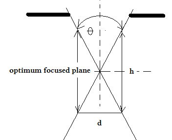
SEM technologytalks about the depth of field which is the distance above and below the plane of optimum focus within which the image is in focus. The focusing of the image is a vital part of a SEM test. In the diagram on the right, d represents the diameter of the electron beam at the specimen. The depth of field is h, since it makes no difference to the sharpness of the image if the object is anywhere within the range h.
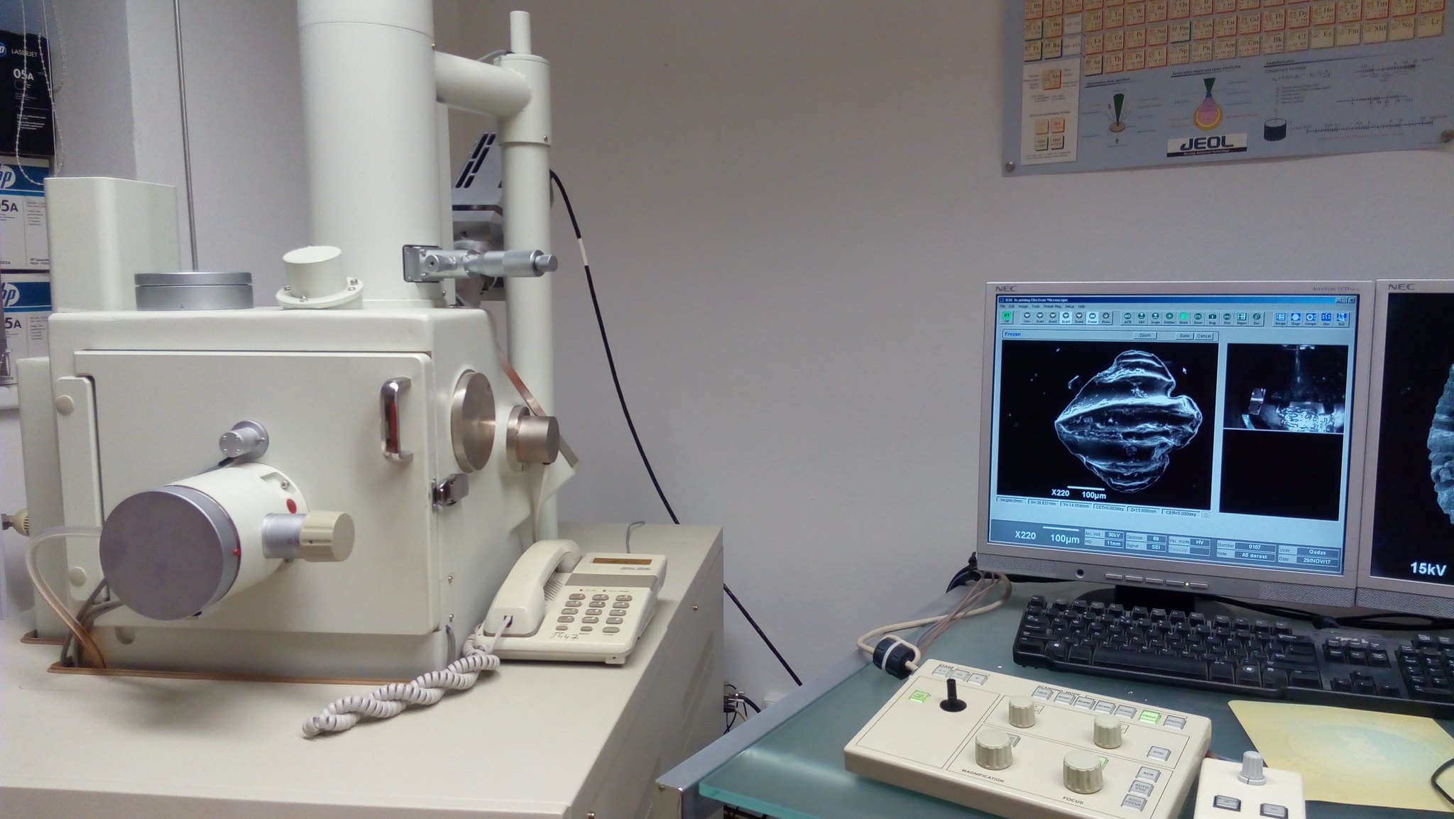
Featured Image – Scanning Electron Microscope(SEM) from Petr Hykš – Flickr